Collaboration Reports and Services
TechSearch International collaborates with several industry leaders that offer reports and services complementary to ours. We work with these partners to jointly develop products that draw upon the strengths and resources of both parties. For example, we team up with SEMI® to produce a comprehensive biennial report on the semiconductor packaging materials market.
Partnership reports and services:
-
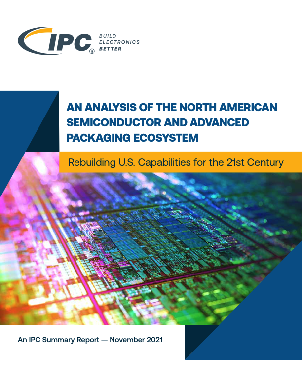
Analysis of the Semiconductor and Advanced Packaging Ecosystem – IPCTechSearch International president Jan Vardaman served as co-author on a study from IPC that provides a thorough, data-driven analysis of the global semiconductor and advanced packaging ecosystem. The study, An Analysis of the North American Semiconductor and Advanced Packaging Ecosystem, highlights the role of advanced packaging in driving innovation in semiconductor designs.
The IPC report makes the case for congressional appropriations of more than $50 billion to support U.S. semiconductor manufacturing, while also underscoring the need to expand advanced packaging capabilities to support the increased production of chips. At a time when the semiconductor supply chain is facing immense pressure, increasing silicon production without bolstering domestic advanced packaging capabilities is likely to lengthen the semiconductor supply chain, as chips will still have to be sent abroad for packaging and assembly into finished products.
Access to the report is free to all. -
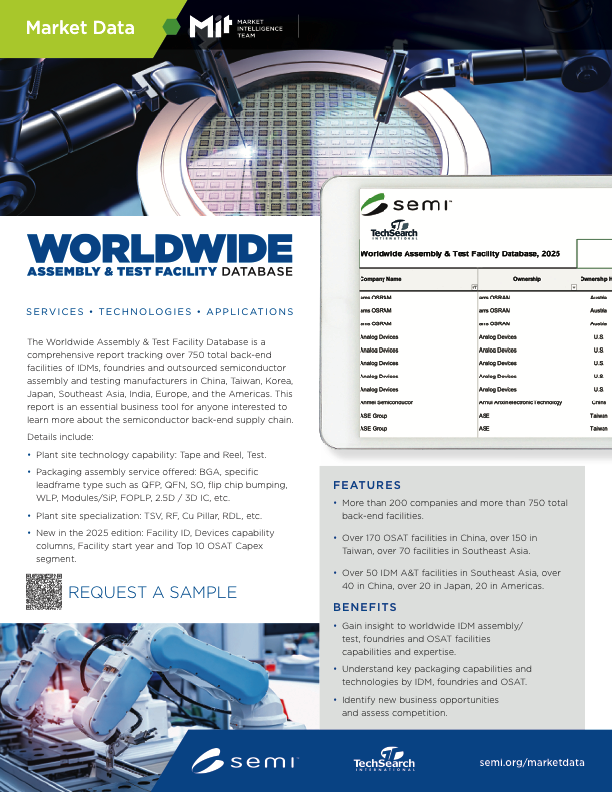
Worldwide Assembly & Test Facility Database (IDM + OSAT), 2025 Edition – SEMI®The Worldwide Assembly & Test Facility Database is a comprehensive report tracking over 750 back-end facilities of IDMs, foundries, and outsourced semiconductor assembly and testing manufacturers in China, Taiwan, Korea, Japan, Southeast Asia, India, Europe, and the Americas. The report is an essential business tool for anyone interested to learn more about the semiconductor back-end supply chain.
Details include:- Plant site technology capability, including Tape and Reel, and Test
- Packaging assembly service offered, such as BGA, Leadframe packages (like QFP, QFN, SO), and Advanced packaging offerings like flip chip bumping, wafer level packaging (WLP), modules/SiPs, FOPLP, 2.5D/3D IC, etc.
- Plant site specializations such as TSV, RF, Cu pillar, RDL, etc.
Key Highlights
- The world's top 20 OSAT companies
- More than 200 companies and over 750 total back-end facilities
- More than 325 facilities with test capabilities
- More than 100 facilities offering QFN
- More than 85 bumping facilities, including more than 65 with 300mm wafer bumping capacity
- More than 90 facilities offering WLCSP technology
- More than 170 OSAT facilities in China, more than 150 in Taiwan, and more than 70 in Southeast Asia
- More than 50 IDM A&T facilities in Southeast Asia, more than 40 in China, more than 20 in Japan, and 20 in Americas
- More than 30% of global factories offer advanced packaging capabilities in one of the following areas: flip chip bumping and assembly, fan-out and fan-in wafer level packaging (WLP), through silicon via (TSV), 2.5D and 3D
Features
- Manufacturing site information
- Packaging technology capabilities
- Plant site applications capabilities
- Type of services offered
- Manufacturing specialization by facility
Benefits
- Gain insight to worldwide IDM assembly/test, foundries, and OSAT facilities capabilities and expertise
- Understand key packaging capabilities and technologies by IDM, foundries, and OSAT
- Identify new business opportunities and assess competition
-
Global Semiconductor Packaging Materials Outlook (2024 Edition) – SEMI®This 2024 edition of the Global Semiconductor Packaging Materials Outlook (GSPMO) is authored by TECHCET and TechSearch International, Inc., in cooperation with SEMI.
The report covers the packaging materials markets, including substrates, lead frames, bonding wire, encapsulation materials, underfill materials, die-attach, solder balls, wafer-level package dielectrics, and wafer-level plating chemicals. However, due to a lack of interest, this report did not include solder balls.
Global Semiconductor Packaging Materials Outlook is an essential business tool for anyone interested in the plastic packaging materials arena. Packaging materials directly affect semiconductors' performance, reliability, and cost, and advancements in packaging materials technology offer the potential for significant improvement across all these areas.Features
- Technology trends
- Regional market size and forecast
- Five-year market forecast to 2028
- Market size by product segments in revenue and units
- Excel workbook file summarizing market information
- Supplier information and market share
Benefits
- Gain insights to worldwide packaging material technology trends, market size, and market forecast
- Learn about market drivers and advancements in packaging materials
- Use benchmark data to validate business opportunities and assumptions
Condensed Table of Contents
- Introduction
- Semiconductor Industry Market Status & Outlook
- Substrates
- Leadframes
- Bonding Wire
- Encapsulation Materials
- Underfill Materials
- Die Attach Materials
- Wafer Level Package Dielectrics
- Wafer Level Plating Chemicals
- Summary and Conclusion
- Appendices
-
Cost Models – SavanSys Solutions
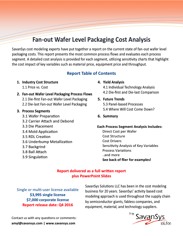
Fan-out Wafer Level Packaging Cost Analysis
Wafer level packaging (WLP) is often the most cost-effective approach for achieving miniaturization. However, using wafer level packaging for the wrong applications can be needlessly expensive. The significant differences between printed circuit board interconnect design rules and semiconductor interconnect design rules must be resolved by the package, and this presents unique challenges for wafer level packaging.
If miniaturization is not required, a wire bond package is usually the most cost-effective packaging approach. However, a modified wafer level packaging approach called fan-out wafer level packaging is one option that overcomes the traditional WLP I/O restrictions. In many cases, fan-out wafer level packaging or flip chip packaging is the lowest cost solution for applications requiring a moderate number of I/Os with some package size constraints.
This paper compares the total packaging cost of the following four technologies:- Wire bond packaging
- Flip chip packaging
- Fan-in wafer level packaging
- Fan-out wafer level packaging
The analysis is accomplished using a comprehensive activity based cost model for each of the four package technologies. All wafer preparation activities (bumping for flip chip, wafer mounting, backgrind, dicing, etc.), fabrication activities (redistribution layer creation, inner layer processing, build-up layer processing, drilling, surface finish, testing, singulation, etc.), and assembly activities (die bonding, wire bonding, underfill, mold compound, lid attach, solder ball attach, etc.) are modeled and verified using multiple industry sources.
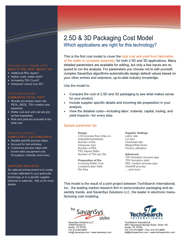
2.5D & 3D Cost Model
After successful collaboration on cost models for Wafer Level Packaging, Flip Chip, Wire Bond, and other technologies, SavanSys Solutions and TechSearch International released a cost trade-off model for 2.5D and 3D packaging technologies. While there are still technical barriers to high volume adoption of 2.5D and 3D packaging solutions, cost remains a primary obstacle. The question is not whether 2.5D and 3D stacks can be built, but rather which applications are appropriate for these technologies based on cost/performance.
The 2.5D & 3D Packaging Cost Model covers the total cost and yield from fabrication of the wafer to complete assembly, for both 2.5D and 3D applications. The user is able to edit a variety of parameters, including TSV and interposer characteristics, supplier specific inputs, and die preparation details. For parameters not known or specified, the model will estimate it based on other user entries and the latest industry knowledge. A detailed cost break down of the total process cost is generated for each analysis, allowing the user to pinpoint the exact steps in the process flow that contribute to cost. In addition, detailed manipulation of the process flow is available, allowing the user to disable or enter specific values for process steps.- SavanSys develops the model software
- TechSearch helps with model calibration
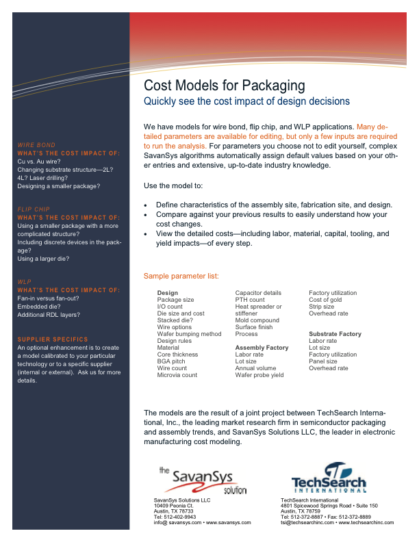
WLP, Flip Chip, Wirebond Cost Models
Wafer level packaging (WLP) is often the most cost-effective approach for achieving miniaturization. However, using wafer level packaging for the wrong applications can be needlessly expensive. The significant differences between printed circuit board interconnect design rules and semiconductor interconnect design rules must be resolved by the package, and this presents unique challenges for wafer level packaging.
If miniaturization is not required, a wire bond package is usually the most cost-effective packaging approach. However, a modified wafer level packaging approach called fan-out wafer level packaging is one option that overcomes the traditional WLP I/O restriction. In many cases, fan-out wafer level packaging or flip chip packaging is the lowest cost solution for applications requiring a moderate number of I/Os with some package size constraints.
This paper compares the total packaging cost of the following four technologies:- Fan-in wafer level packaging
- Fan-out wafer level packaging
- Flip chip packaging
- Wire bond packaging
The analysis is accomplished using a comprehensive activity based cost model for each of the four package technologies. All wafer preparation activities (bumping for flip chip, wafer mounting, backgrind, dicing, etc.), fabrication activities (redistribution layer creation, inner layer processing, build-up layer processing, drilling, surface finish, testing, singulation, etc.), and assembly activities (die bonding, wire bonding, underfill, mold compound, lid attach, solder ball attach, etc.) are modeled and verified using multiple industry sources.- SavanSys develops the model software
- TechSearch helps with model calibration
-
System Teardown Reports – TPSS GroupIn addition to performing our own teardowns of leading-edge system products, TechSearch International also markets teardown reports from Total Process Solution Study Group (TPSS) in Japan.

Who We Are
TechSearch International is recognized around the world as a leading consulting company in the field of advanced semiconductor packaging and assembly, electronics manufacturing, and materials.
Network

Contact
- email message
- +1.512.372.8887
- +1.512.372.8889
- 4801 Spicewood Springs Rd, Ste 150
Austin, TX 78759
United States
Copyright © 2015–2026 TechSearch International, Inc. • techsearchinc.com • all rights reserved