Volume 2-0718

July 2018
order form
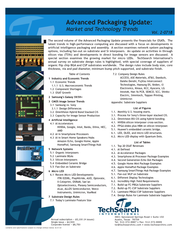
This issue of the Advanced Packaging Update presents the current state of outsourced semiconductor assembly and test (OSAT) financials. The latest trends in high-performance computing are discussed with a focus on developments in artificial intelligence packaging and assembly. An update on activities in through silicon vias (TSVs) and developments in direct bonding are discussed. A special section examines the growing market for micro LEDs. TechSearch International’s annual survey on substrate design rules is highlighted, with special coverage of suppliers of organic flip chip BGA and CSP substrates worldwide. The design rules include body size, core thickness, via and pad diameter, minimum bump pitch supported, and substrate finish.
  • Contents…
    • 1 Industry and Economic Trends
      • 1.1 Economic Trends
        • 1.1.1 U.S. Macroeconomic Trends
      • 1.2 Component Shortages
      • 1.3 OSAT Growth
    • ​2 Samsung's Galaxy S9/S9+
    • 3 CMOS Image Sensor Trends
      • 3.1 Samsung vs. Sony
        • 3.1.1 Design Differences
      • 3.2 OmniVision Hybrid Bond Stack CIS
      • 3.3 Capacity for Image Sensor Production
    • 4 Artificial Intelligence
      • 4.1 AI Accelerators
        • 4.1.1 NVIDIA
        • 4.1.2 Google
        • 4.1.3 Intel
        • 4.1.4 Baidu
        • 4.1.5 Xilinx
        • 4.1.6 NEC
        • 4.1.7 AMD
      • 4.2 AI in Smartphone Processors
      • 4.3 AI in Smart Home Speakers/Hubs
        • 4.3.1 Amazon Echo
        • 4.3.2 Google Home
        • 4.3.3 Apple HomePod
        • 4.3.4 Samsung SmartThings Hub
    • 5 Network Systems
      • 5.1 Organic Interposers
      • 5.2 Laminate BGAs
      • 5.3 Silicon Interposers
      • 5.4 Embedded Ceramic Bridge
      • 5.5 Fan-Out on Substrate
    • 6. Micro LED
      • 6.1 ​Recent Micro LED Developments
        • 6.1.1 ITRI EOSRL
        • 6.1.2 PlayNitride
        • 6.1.3 AUO
        • 6.1.4 Optovate
        • 6.1.5 X-Celeprint and OSRAM
        • 6.1.6 San'an Optoelectronics
        • 6.1.7 Plessey Semiconductors
        • 6.1.8 eLux
        • 6.1.9 ALLOS Semiconductor and Veeco Instruments
        • 6.1.10 Unimicron
        • 6.1.11 VueReal
    • 7 Substrate Design Rules
      • 7.1 Today's Laminate Feature Size
      • 7.2 Company Design Rules
        • 7.2.1 ACCESS Semiconductor
        • 7.2.2 ASE Materials
        • 7.2.3 AT&S
        • 7.2.4 Daeduck
        • 7.2.5 Daisho Denshi
        • 7.2.6 Fujitsu Interconnect Technologies
        • 7.2.7 Haesung DS
        • 7.2.8 Ibiden
        • 7.2.9 i3 Electronics
        • 7.2.10 Kinsus Interconnect Technology
        • 7.2.11 Korea Circuit Company
        • 7.2.12 Kyocera
        • 7.2.13 LG Innotek
        • 7.2.14 Nan Ya PCB
        • 7.2.15 Samsung Electro-Mechanics
        • 7.2.16 Shennan Circuits
        • 7.2.17 Shinko Electric
        • 7.2.18 Simmtech
        • 7.2.19 Toppan Printing
        • 7.2.20 Unimicron Technology
    • Appendix: Substrate Suppliers
    • References
  • Figures…
    • 1.1 Monthly U.S. housing starts.
    • 3.1 Process flow for Sony's three-layer stacked CIS.
    • 3.2 OmniVision BSI CIS using hybrid bonding stacking.
    • 4.1 NVIDIA silicon interposer package cross-section.
    • 4.2 FPGA slides plus HBM on silicon interposer.
    • 5.1 Huawei's embedded ceramic bridge.
    • 6.1 LED, OLED, and micro LED structures.
    • 6.2 Micro LED display with Quantum Dots.
  • Tables…
    • 1.1 Top 20 OSAT Revenues
    • 4.1 AI Defined
    • 4.2 AI Accelerator Packages
    • 4.3 Smartphone AI Processor Package Examples
    • 4.4 Second Generation Echo Dot Package Examples
    • 4.5 Google Home Mini Package Examples
    • 4.6 Apple HomePod Package Examples
    • 4.7 Samsung SmartThings Hub Package Examples
    • 5.1 Fan-out WLP on Substrate
    • 6.1 Specifications of Different Display Technologies
    • 6.2 Incredibly High Yield Requirements
    • 7.1 Selected Build-up FC-PBGA Substrate Suppliers
    • 7.2 Selected Build-up FC-CSP Substrate Suppliers
    • 7.3 Selected Laminate PBGA/CSP Substrate Suppliers
    • 7.4 Design Rules for ACCESS Coreless Substrates
    • 7.5 Design Rules for ACCESS FC-CSP Substrates
    • 7.6 Design Rules for ACCESS Wire Bond CSP Substrates
    • 7.7 Design Rules for ASE PBGA/CSP Substrates
    • 7.8 Design Rules for AT&S FC-PBGA Substrates
    • 7.9 Design Rules for Daeduck FC-CSP Substrates
    • 7.10 Design Rules for Daeduck Thin Build-Up WB Substrates
    • 7.11 Design Rules for Daisho Denshi PBGA/CSP Substrates
    • 7.12 Design Rules for FICT FC-PBGA Substrates
    • 7.13 Design Rules for Ibiden FC-PBGA Substrates
    • 7.14 Design Rules for Ibiden FC-CSP Substrates
    • 7.15 Design Rules for Ibiden Coreless Substrates
    • 7.16 Design Rules for CoreEZ® Substrates
    • 7.17 Design Rules for HyperBGA® Substrates
    • 7.18 Design Rules for i3 Electronics PBGA Substrates
    • 7.19 Design Rules for MicroFlex (Polyimide)
    • 7.20 Design Rules for Kinsus FC-PBGA Substrates
    • 7.21 Design Rules for Kinsus FC-CSP Substrates
    • 7.22 Design Rules for Kinsus PBGA/CSP Substrates
    • 7.23 Design Rules for Kinsus Coreless Substrates
    • 7.24 Design Rules for Korea Circuit Company FC-CSP Substrates
    • 7.25 Design Rules for Korea Circuit Company PBGA Substrates
    • 7.26 Design Rules for Kyocera FC-PBGA Substrates
    • 7.27 Design Rules for Kyocera FC-CSP Substrates
    • 7.28 Design Rules for Kyocera Coreless Substrates
    • 7.29 Design Rules for LG Innotek CSP Substrates
    • 7.30 Design Rules for LG Innotek FC-CSP Substrates
    • 7.31 Design Rules for Nan Ya PCB FC-PBGA Substrates
    • 7.32 Design Rules for Nan Ya PCB PBGA/CSP Substrates
    • 7.33 Design Rules for Nan Ya PCB FC-CSP Substrates
    • 7.34 Design Rules for Nan Ya PCB Coreless Substrates
    • 7.35 Design Rules for SEMCO FC-PBGA Substrates
    • 7.36 Design Rules for SEMCO PBGA/CSP Substrates
    • 7.37 Design Rules for SEMCO FC-CSP Substrates
    • 7.38 Design Rules for SCC PBGA/CSP Substrates
    • 7.39 Design Rules for Shinko Electric FC-PBGA Substrates
    • 7.40 Design Rules for Shinko Electric FC-CSP Substrates
    • 7.41 Design Rules for Shinko Electric Coreless Substrates
    • 7.42 Design Rules for Shinko Electric PBGA/CSP Substrates
    • 7.43 Design Rules for Simmtech PBGA/CSP Substrates
    • 7.44 Design Rules for Simmtech Coreless Substrates
    • 7.45 Design Rules for Toppan FC-PBGA Substrates
    • 7.46 Design Rules for Toppan Coreless Substrates
    • 7.47 Design Rules for Unimicron FC-PBGA Substrates
    • 7.48 Design Rules for Unimicron FC-CSP Substrates
    • 7.49 Design Rules for Unimicron PBGA/CSP Substrates
Stacks Image 25201
brochure
  • Published July 2018
  • 86 pages
  • 8 figures / 60 tables
  • 46 PowerPoint slides
  • $5,100 annual subscription (4 issues)
    $2,500 single issue
    $8,750 corporate license
Who We Are
TechSearch International is recognized around the world as a leading consulting company in the field of advanced semiconductor packaging and assembly, electronics manufacturing, and materials.
Network
Contact
  • email message
  • +1.512.372.8887
  • +1.512.372.8889
  • 4801 Spicewood Springs Rd, Ste 150
    Austin, TX 78759
    United States